 Pin
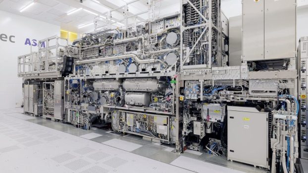
Pin ASML’s TWINSCAN EXE:5000 pushes the boundaries of next-gen chip production. Image credit: ASML
Buried inside ultra-secure Dutch labs, a single company holds the blueprint to modern computing. ASML’s invention isn’t just a machine—it’s the gatekeeper of every breakthrough in artificial intelligence today. With governments lining up and tech giants whispering deals in boardrooms, all eyes quietly turn to one place: Veldhoven, Netherlands.
The ASML Netherlands AI chip making machine doesn’t look like science fiction. But its impact? World-altering. Using beams of extreme ultraviolet light, it prints circuitry so small, human eyes can’t detect it. Each chip it helps produce becomes the brain of AI systems that are now predicting weather, detecting cancer, and piloting drones.
This machine isn’t sold in bulk. Only a handful are made each year. And only the most powerful nations and companies can afford one. The question isn’t who uses it. The real question is—who controls it? Because whoever does, controls the future of AI, and maybe, everything else.
Table of Contents
The Minds Behind the Machine That Changed Everything
The story of ASML’s groundbreaking chip machine isn’t about one lone genius—it’s a saga of collaboration, vision, and relentless engineering. ASML itself was founded in 1984 as a joint venture between Philips and ASM International, starting in a small shed next to a Philips building in Veldhoven. Few could have guessed it would one day become the beating heart of global chipmaking.
The EUV lithography breakthrough—the core of the ASML machine—was driven by decades of work from engineers and physicists across Europe, Japan, and the U.S. Key contributions came from Dutch scientists at ASML, optical experts at Germany’s ZEISS, and laser innovators at America’s Cymer. There was no “Eureka!” moment—just tireless problem-solving, where breakthroughs came one impossible task at a time.
Among the many names etched into this story is Martin van den Brink, ASML’s long-time CTO and now Vice Chair. His leadership helped transform the dream of EUV into reality, leading teams that made light bend to human will. It’s a legacy written not in textbooks—but etched onto the silicon powering the AI revolution.
Why No One Else Can Copy ASML’s Masterpiece
There’s a reason no rival has been able to catch up. ASML’s technology isn’t just difficult—it’s borderline impossible to replicate. The chip making machine depends on something called EUV lithography, a technique so advanced that it took decades of trial, error, and obsession to perfect. Without it, the latest AI chips wouldn’t even exist.
Only ASML cracked the code. It’s not just about patents or money—it’s about rare partnerships and extreme specialization. Over 800 suppliers and thousands of engineers contribute to each machine, making it a global effort no single nation can reproduce on its own. Even if someone tried, they’d face physics problems no textbook can solve.
This isn’t like building a smartphone or a car. It’s like recreating a miracle. That’s why the world waits in line—because ASML builds the only doorway into the future of AI. And with only a few machines produced each year, owning one is like holding a golden ticket to control tomorrow’s technology.
How Does ASML Keep This Wonder Machine in Motion?
ASML doesn’t work alone in powering its extraordinary chipmaking marvel. Over 5,000 global suppliers funnel specialized parts—like ultra-precise mirrors from ZEISS, molten tin plasma systems, and vibration-free stages—into each machine. These devices weigh nearly 200 tons and need three Boeing 747s just for transport. Every machine is a testament to coordination, precision, and innovation.
Maintaining these machines requires elite engineers like Brienna Hall, one of roughly 10,000 globally trained specialists. In labs cleaner than operating theaters, they troubleshoot features finer than human hair—some wear cleanroom suits to prevent even a single particle from disrupting production. ASML also built a new training center in Arizona, aiming to train 1,200 engineers yearly to support this complex infrastructure.
Yet complexity comes with scarcity. ASML produced just around 40 EUV machines last year, with orders stretching years ahead. High-NA models are even more limited: only six a year globally, each costing roughly $370 million. That’s why owning one is like possessing a key to the most advanced realms of AI research and chipmaking — and why every moment of uptime counts.
The High-Stakes Race Around High‑NA EUV
ASML has already delivered its first High‑NA (0.55 NA) EUV machines—for research and pilot production—to top chipmakers like Intel and TSMC. These towering machines weigh around 150–180 tons, need three Boeing 747s for transport, and come with a jaw-dropping price tag of $370–$380 million each. Imagine a piece of equipment so massive and expensive that owning one feels like holding a nation’s semiconductor future in your hands.
Intel seized all of ASML’s High‑NA output in 2024—five or six units—and put them to work in Oregon R&D labs. By late 2023, its trial system had processed tens of thousands of wafers in a single quarter, showing they could replace multi‑step exposures with one high‑precision pass. While this is groundbreaking, full production versions won’t roll out until 2026–2027.
Others are watching closely. ASML already booked 10–20 initial orders and plans to make 20 High‑NA systems annually by 2028. But adoption will vary—Intel is going all-in first, while TSMC and Samsung are taking a slower, cautious approach . From labs to full-scale fabs, the world is witnessing a high-stakes countdown. Who joins the High‑NA club next could shape the chip landscape for the next decade.
The Global Chess Match Around High‑NA Deployment
The unveiling of High‑NA systems sparks a strategic dance across semiconductor giants. TSMC remains cautious, evaluating cost versus benefit before embracing one of ASML’s most potent tools . Intel, by contrast, has already secured ASML’s full 2024 output—five systems—and is pioneering their use in future production lines . Samsung and SK Hynix wait in line, aware that supply is limited and timing is vital.
Analysts warn the next few years could be rocky. Barclays forecasts only three High‑NA shipments in 2026, echoing whoosh of slowing commitments from Samsung and Intel . Still, ASML has 10–20 orders booked and plans to scale to 20 units annually by 2028 . If adoption accelerates, the company could face a capacity crunch—or a surge in pricing power.
For chipmakers, this is more than a technology decision—it’s strategy. Those who adopt early stand to streamline complex processes and gain performance edges. Those who wait might save cost—but risk falling behind. The High‑NA era isn’t just a technical upgrade. It’s a high-stakes gamble on who will shape the next decade of AI and computing power.
Navigating Supply Chains, Geopolitics & Tomorrow’s Tools
ASML wears its monopoly crown, but that crown is heavy. Nearly 85% of its machine components come from outside—some crucial parts from single suppliers like Zeiss optics or Cymer laser firms . A hiccup in any link—trade restrictions, factory fire, political turmoil—can delay production by months. It’s a microcosm of modern manufacturing: global in design, fragile in execution. ASML’s agility depends on managing this sprawling, delicate ecosystem, or facing halted shipments and millions in lost revenue.
U.S.–China tensions tense up the equation. The Biden administration currently bars ASML from exporting its most powerful EUV tools to China—a move aimed at tech containment . In Asia, hub governments are pushing chip capabilities at home, but without ASML’s Extreme UV lithography, local players face an uphill climb . Meanwhile, ASML aims to spread production by opening training centers in Arizona and test labs in Europe, but scaling this global talent is proving as tough as the machines themselves.
Looking ahead, the company is chasing even more ambitious tech. High‑NA EUV tools are just the tip—Hyper‑NA systems could arrive by 2030, pushing resolution below 1.5nm . Yet every step forward brings complexity: new masks, tougher optics, steeper costs, and energy demands. In this high-stakes gamble, ASML must stay ahead of physics, politics, and partnerships to carve the path for the next decade of AI innovation.
The Social, Economic, and Technological Ripple Effects of ASML's Innovation
ASML’s dominance in EUV lithography isn’t just a tech story—it’s reshaping entire industries and economies. In collaboration with cultural institutions like the Van Gogh Museum, the company adapts its nanometer‑scale imaging tools to digitally preserve priceless art, transforming chips into custodians of culture . When one enterprise’s breakthrough can conserve global heritage, we see how deep the reach of semiconductor innovation really runs.
Financial markets are taking notice too. ASML forecasts revenue rising to €60 billion by 2030, driven by booming AI demand. That impressive outlook helped send its stock up 2.9%, even amid broader market pressures. Investors understand this: mastering EUV means more than leveraging Moore’s Law—it means owning the gateway to AI’s future.
The ripple effect spreads to geopolitics and supply chains. US export controls have blocked ASML’s most advanced tools from reaching China, giving Western chipmakers a strategic edge. Meanwhile, Chinese firms scramble to develop domestic alternatives—and analysts stress that optics from Germany’s Zeiss remain irreplaceable. ASML’s technological edge is therefore a catalyst—powering industries, markets, politics, and even culture—proving that mastering the microscopic can shift the global landscape.
How ASML’s Tiny Tech is Shaping Culture, Economy & Geopolitics
In an unexpected twist, ASML’s precision machines are preserving art. Inside the Van Gogh Museum, a nanometer‑level scanner—born from chip metrology—captures the thick, dramatic brushstrokes in 3D at gigabyte volume. It’s like creating a “Google Maps for paintings,” digitally immortalizing masterpieces with unmatched depth and detail . This tool isn’t for chips—it’s cultural stewardship, redefining how we preserve and interact with centuries‑old artwork.
On the financial stage, ASML forecasts €44–60 billion in revenue by 2030, thanks to relentless AI demand . After booking €7 billion orders in Q4, its stock jumped 11%, reflecting investor confidence in the chip-innovation boom . This impressive growth isn’t just numbers—it reflects a shift where semiconductor mastery equals global economic power, and ASML sits at its center.
But technology and money aren’t the whole story. Export controls, especially U.S.–Dutch limits on shipping EUV tools to China, are reshaping global power balances . Governments race to build domestic chip industries—but without ASML’s technology, they’re climbing uphill. ASML’s machines have become geopolitical leverage: instruments of innovation, shields of sovereignty, and bridges between science, culture, and global strategy.
The Human Factor Inside ASML’s Fortress of Innovation
Behind every beam of light and billion-dollar contract is a workforce built on discipline, creativity, and trust. ASML employs over 40,000 people across the globe, but the heart of its operation beats in Veldhoven. Engineers there work in cleanrooms more sterile than hospital operating theaters. Wearing full-body suits, they guide beams thinner than a virus through machines the size of small houses.
Recruiting and retaining talent at this level isn’t easy. ASML competes with the biggest names in tech, yet it’s not headquartered in Silicon Valley or Shenzhen—it’s in a small Dutch town. To attract elite minds, it invests heavily in training, housing support, and international relocation. A new Arizona training center aims to mold 1,200 engineers per year, prepping them for the high-pressure world of EUV systems.
But it’s not just about skill—it’s about passion. ASML insiders speak of obsession, of solving problems no one’s cracked before. Some describe it as an engineering temple. For these minds, it’s not just a job—it’s a mission to shape the technology that will define the next century.
What the Future Holds for ASML and the World of AI Chips
As the world races toward smaller, faster, and more powerful AI chips, ASML is already preparing for what comes next. While High-NA EUV machines are still rolling out, the company is exploring Hyper-NA lithography. This would push chip production to sub-1.5nm levels—beyond what current physics comfortably allows. It’s no longer just engineering; it’s a challenge to nature itself.
Such progress doesn’t come cheap or easy. Hyper-NA machines will require new photoresist chemicals, stronger laser sources, and even more advanced optical systems. The cost per machine could top half a billion dollars. Still, leading chipmakers are watching closely. Because with each advance, ASML offers something no one else can: access to computing power that redefines industries.
In this next phase, ASML won’t just be a supplier—it will be a gatekeeper to the post-silicon era. As AI expands into every corner of life, from medicine to finance to defense, ASML’s role will only deepen. The question now is: how far ahead can they stay—and who, if anyone, can catch up?
FAQs
The ASML Netherlands AI chip making machine is the only tool in the world that can produce advanced chips using extreme ultraviolet (EUV) lithography. These chips power today’s most powerful AI systems, from language models to autonomous vehicles. Without ASML’s machine, no company—regardless of size—can build the cutting-edge processors AI depends on.
ASML’s EUV machines operate on a completely different level of precision. They use light waves just 13.5 nanometers wide to print intricate circuits that are invisible to the human eye. This allows chips to pack more power into smaller spaces—something no other company has managed at this scale. It’s a blend of advanced physics, optics, and materials science.
No company has been able to replicate ASML’s EUV technology. It took over 20 years of research, thousands of engineers, and partnerships with specialized firms like Zeiss to reach this level. Even well-funded competitors struggle with the technical barriers. ASML remains the only source for these machines globally.
Due to national security concerns, the U.S. and Dutch governments have imposed export restrictions on ASML, preventing it from shipping its most advanced tools to China. The fear is that these machines could help China leap ahead in AI and military technology. This has turned ASML into a key player in geopolitical strategy.
High‑NA EUV is the next evolution in chipmaking. It uses a larger numerical aperture (NA) lens system, allowing for even finer circuit patterns. This means future chips can be faster and more energy-efficient. Intel is leading the way in adopting this technology, while others like TSMC and Samsung are watching the results closely before diving in.


